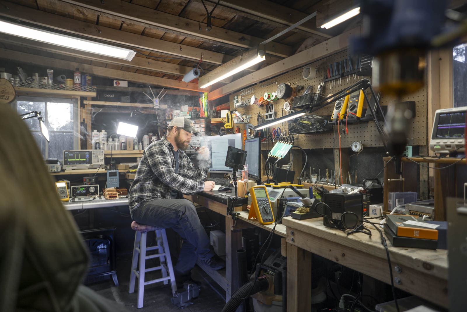
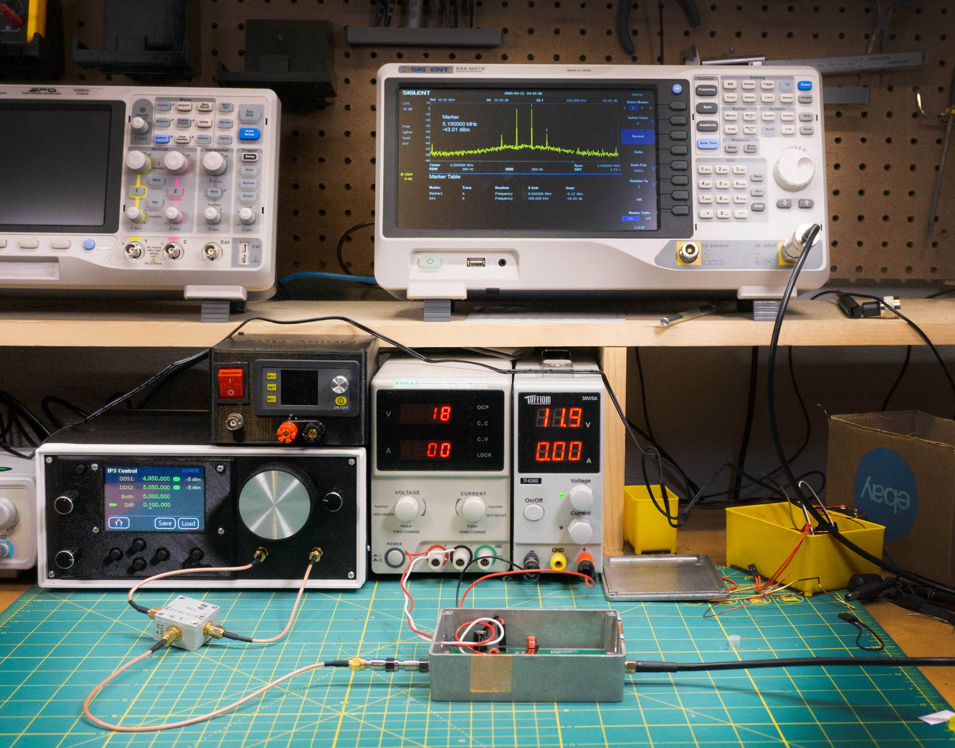
This is my temporary lab in Colorado. Just moved back from Ohio and waiting to close on our house. This setup is in my parents back yard…
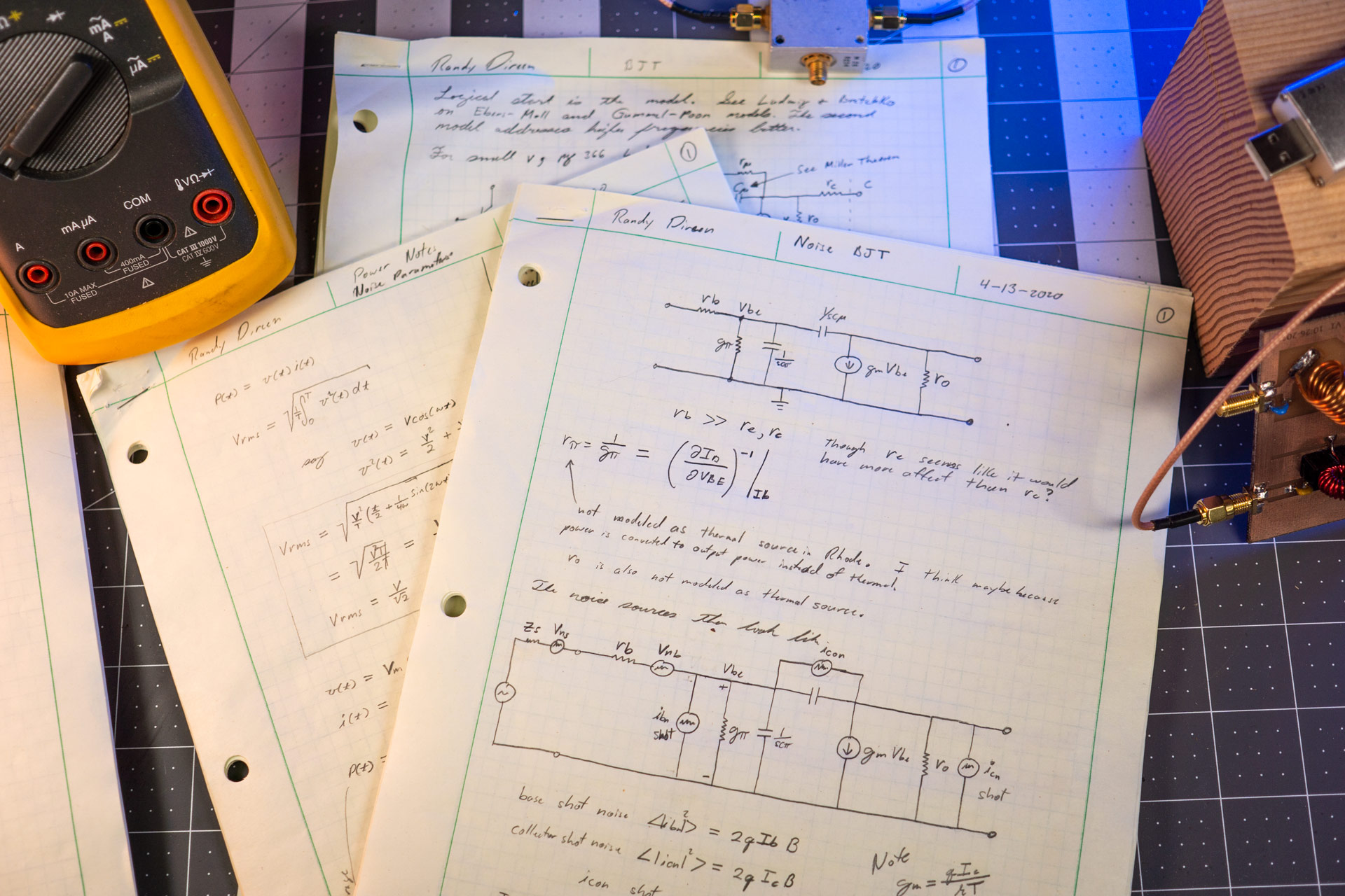
In my down time I’m studying noise in BJTs. I have a handful of papers I’m using for reference (TODO: put references in).
My wife helped me write a bunch of MATLAB routines to work with covariance matrices. I now how a pretty powerful setup to simulate RF noise parameters. I’ll report on those here soon.
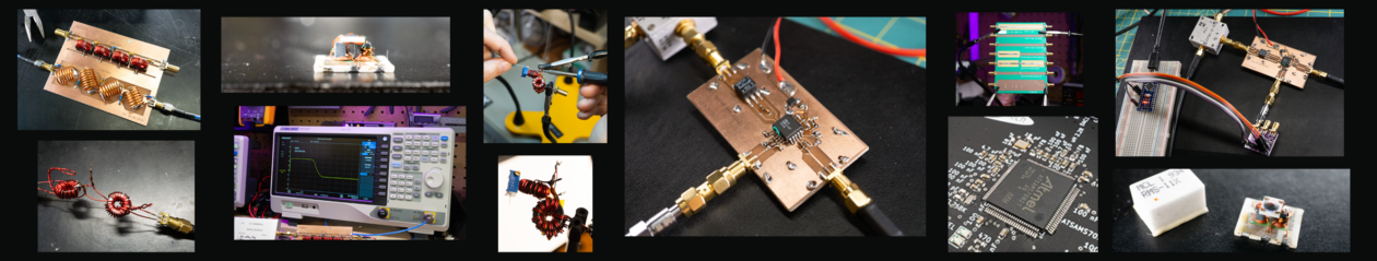
This post is about testing the RF measurement bench I’ve been making. I now have a DIY kit to make noise figure measurements, and a DIY signal generator to make TOI measurements. These along with my KC901V Chinese network analyzer and my Siglent spectrum analyzer provided me with a lot of DIY power.
The image above is a board I had made to test common emitter amplifier configurations. It has room for biasing components, degeneration components, a few places for matching components and exposed metal where I can solder in anything else I want. I made 10 of these for about $30 (ordered from JLCPCB). I have a booklet of 0805 resistors and capacitors I bought off of Amazon, as well as a bunch of wire for making inductors.
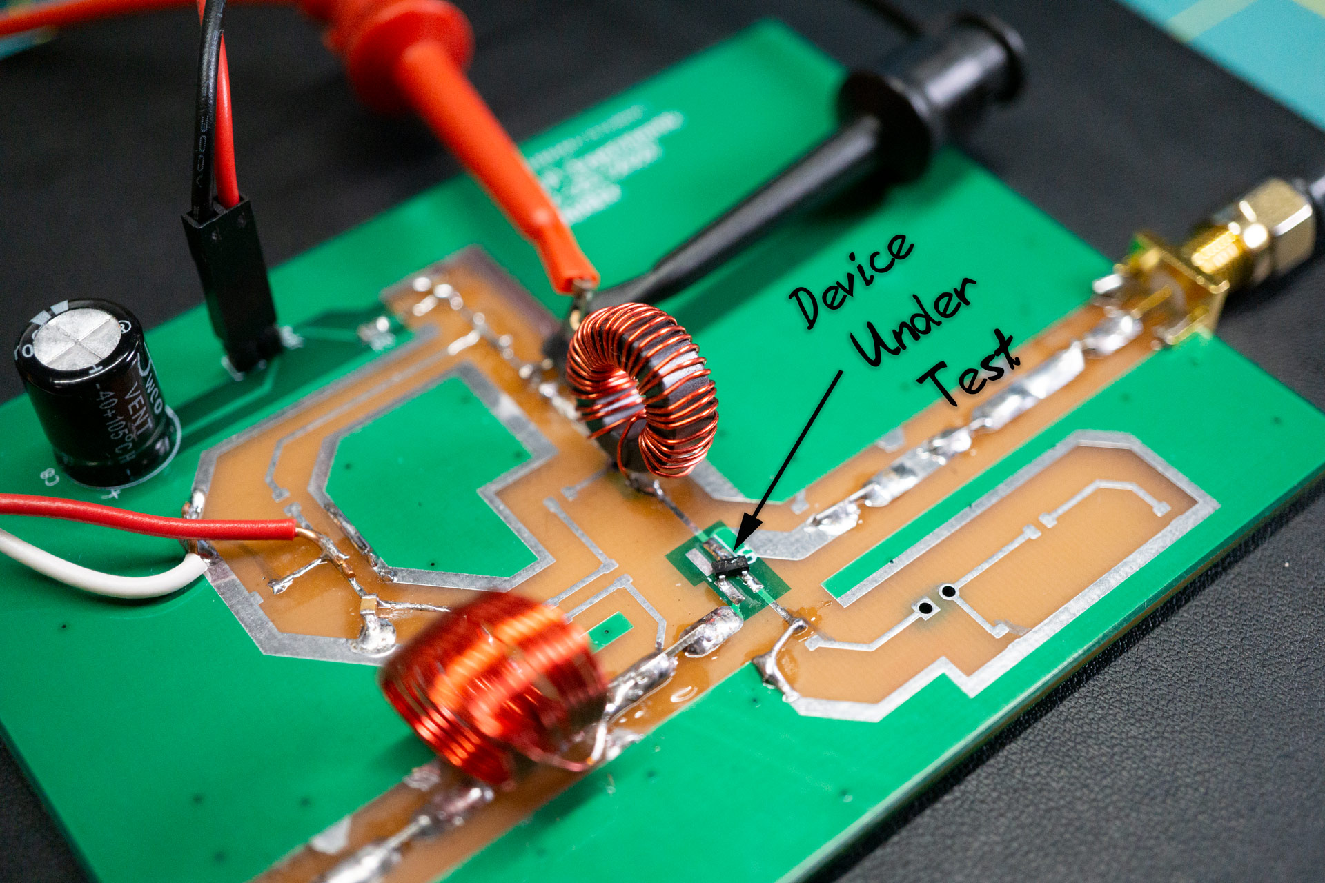
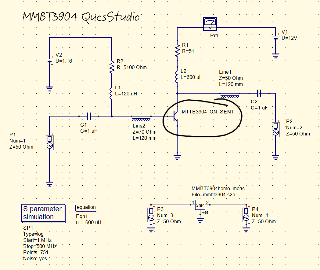
The device I tested is a MMBT3904. No matching, no feedback, no degeneration. Just a couple bias tees and transmission lines. The QucsStudio design shown above provides the values I used for the experiment. I used V2 to test a couple biasing points (20ish mA and 40ish mA).
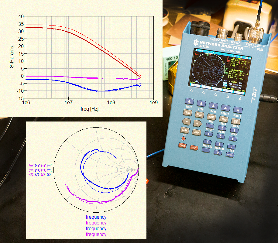
I used my KC901V Chinese network analyzer to measure the S-Parameters and then compared them with simulated results. The thick lines in the plots above are the measurements, and the thin are simulated with QucsStudio. I had to alter RB and CJC in the MMBT3904 Spice model to get the measurement to line up with simulation. Doing so made things line up nicely, but I’m not sure it exactly corresponds with what’s going on. Since I’m just playing, I didn’t spend too much time thinking about it. Good enough for who it’s for.
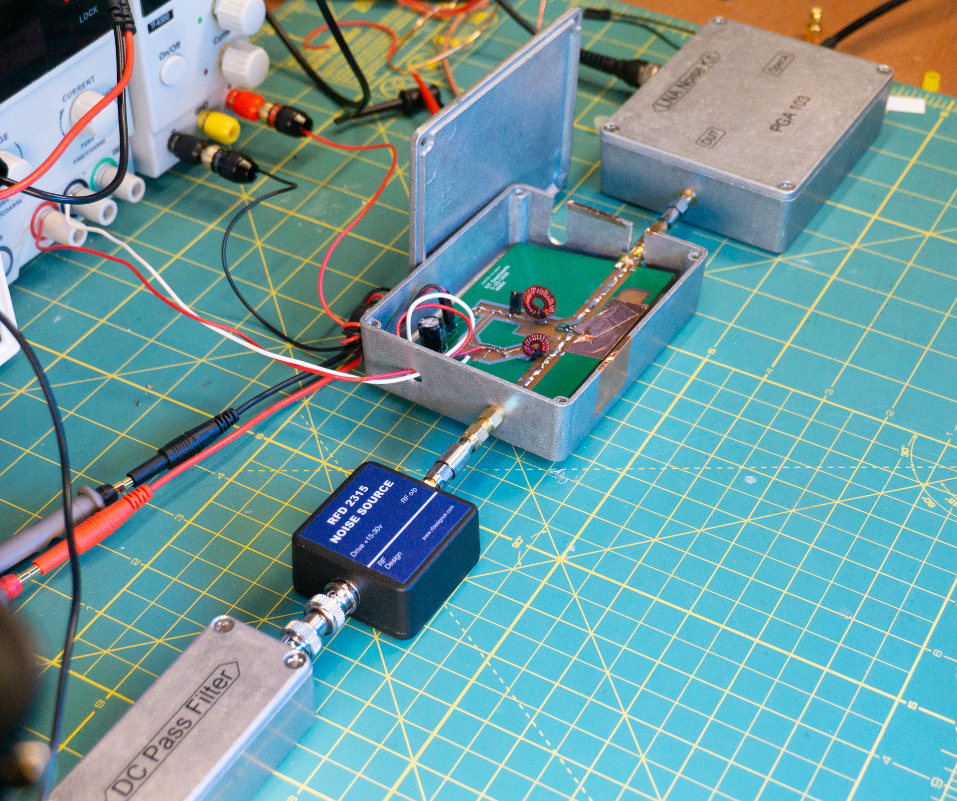
Next I measured noise figure. The setup seen below is the kit I built for measuring noise with my Siglent spectrum analyzer. At the bottom of the image you see the calibrated noise source from RF Design. It has an ENR of 15 dB and is calibrated from 10 MHz to 1420 MHz. The top of the screen shows a box containing a 25 dBish LNA to set the noise floor and add some gain going into the spectrum analyzer.
When I made the common emitter circuit board, I designed it so I could easily stuff it into the aluminum box shown above. I buy these from Amazon and like to use them for RF project boxes. For noise figure measurements you really need to do something like this; otherwise, environmental noise easily corrupts the measurement.
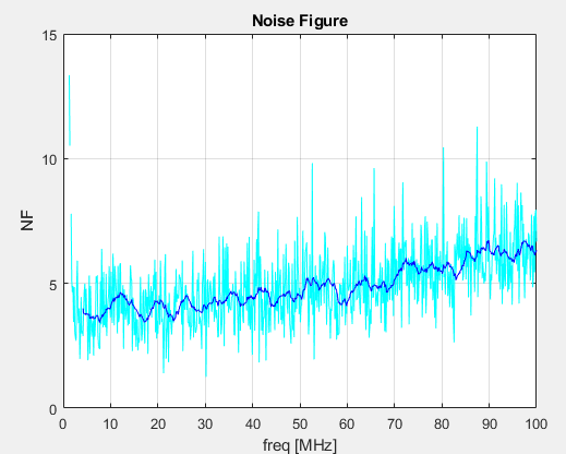
For the measurement I use MATLAB to control the spectrum analyzer. MATLAB places the analyzer into the correct state and collects data over the limits I specify. Using the ENR of the noise source, I calculate noise figure via the Y-Factor method. I’ve had to spend time getting this right, but I believe the figure above is correct to within 1 dB… or two. There are many places where uncertainties creep into these measurements and I’m still working on understanding the limits of this setup. But, the datasheet for the MMBT3904 does say its noise figure is 5 dB. It does not specify the minimum NF, so I’m not sure how small it can be. (Stay tuned in future posts where I make a noise figure parameters measurement DIY kit 😐 .)
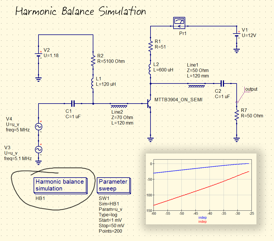
The final measurement I made was of the TOI using my new signal generator. I built this box and wrote about it in a previous post. The box can be seen in the lower left side of the image below. I made it so I could easily generate a couple tones for doing IP3 measurements. (It also does other stuff.)
The OIP3 value I measured was about 21 dB. To verify, I used Harmonic Balance analysis in QucsStudio:
Harmonic Balance Simulation
Aaaand the result is OIP3 = 20.9 dB. Usually when simulation and measurement are this close I’m more suspicious than if the results were wildly off. But, since this was just an exercise in testing out my RF measurement bench, I’m going to call it a day.
Right now I’m really happy with this setup. I’ll continue ironing out problems and reducing uncertainties as I work on more projects.
A signal generator made for controlling a dual conversion HF front-end and for making IP3 measurements. Here are some specs:
Generates two sine waves. One for each SMA port.
Frequency range from 500 KHz up to 150 MHz.
Power from -99 dBm to -5 dBm.
Controls for setting up two tone measurements.
Controls for tuning a dual conversion HF front-end.
That’s it.
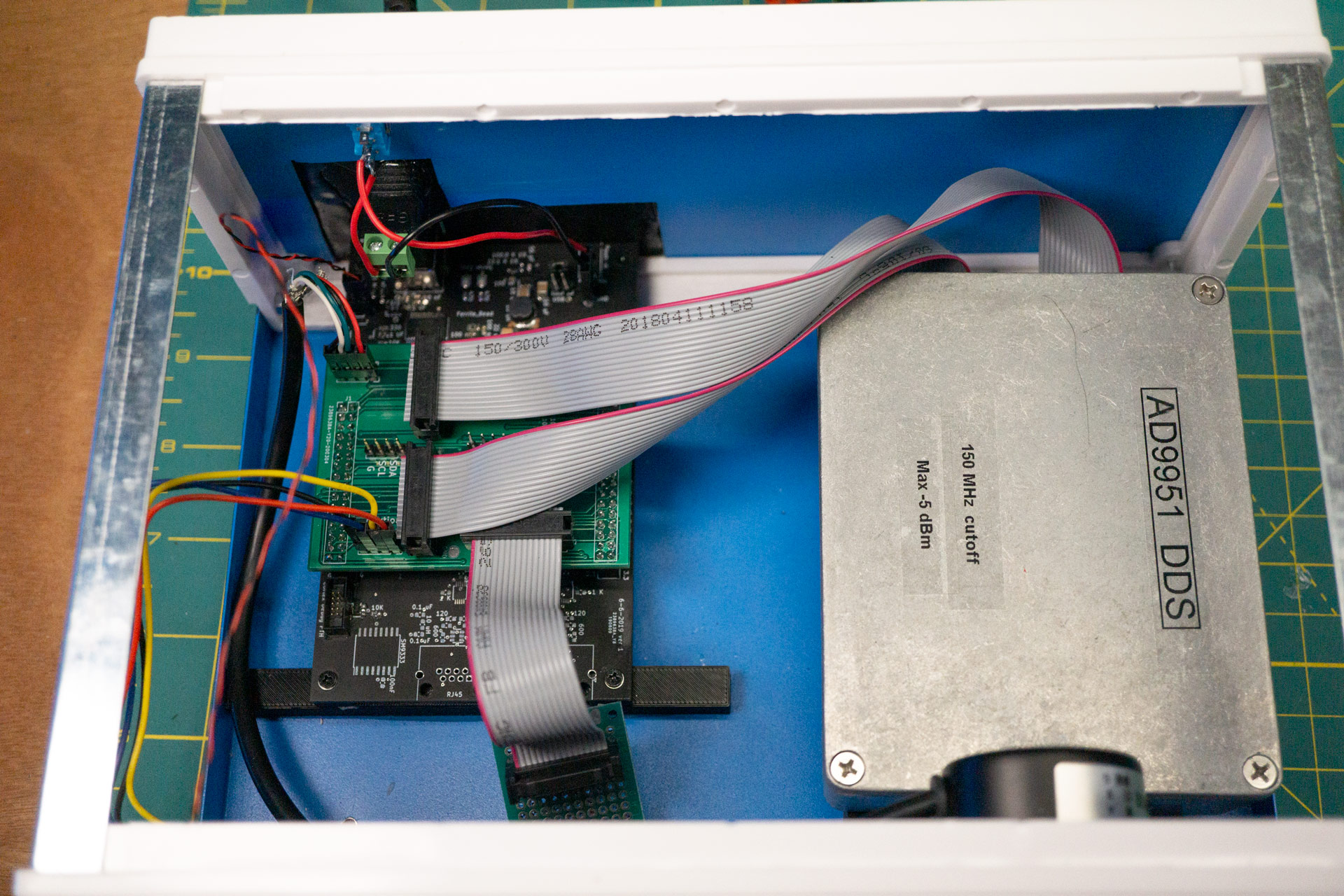
The generator is made up of a bunch of stuff I’ve been playing with. There are two AD9951 DDS chips for synthesizing signals (see below). There is a 300 MHz Atmel M7 chip on a board my dad and I built last year. The display is a 3.5″ Enhanced Nextion screen. And everything else I bought on Amazon or eBay.
AD9951 DDS board
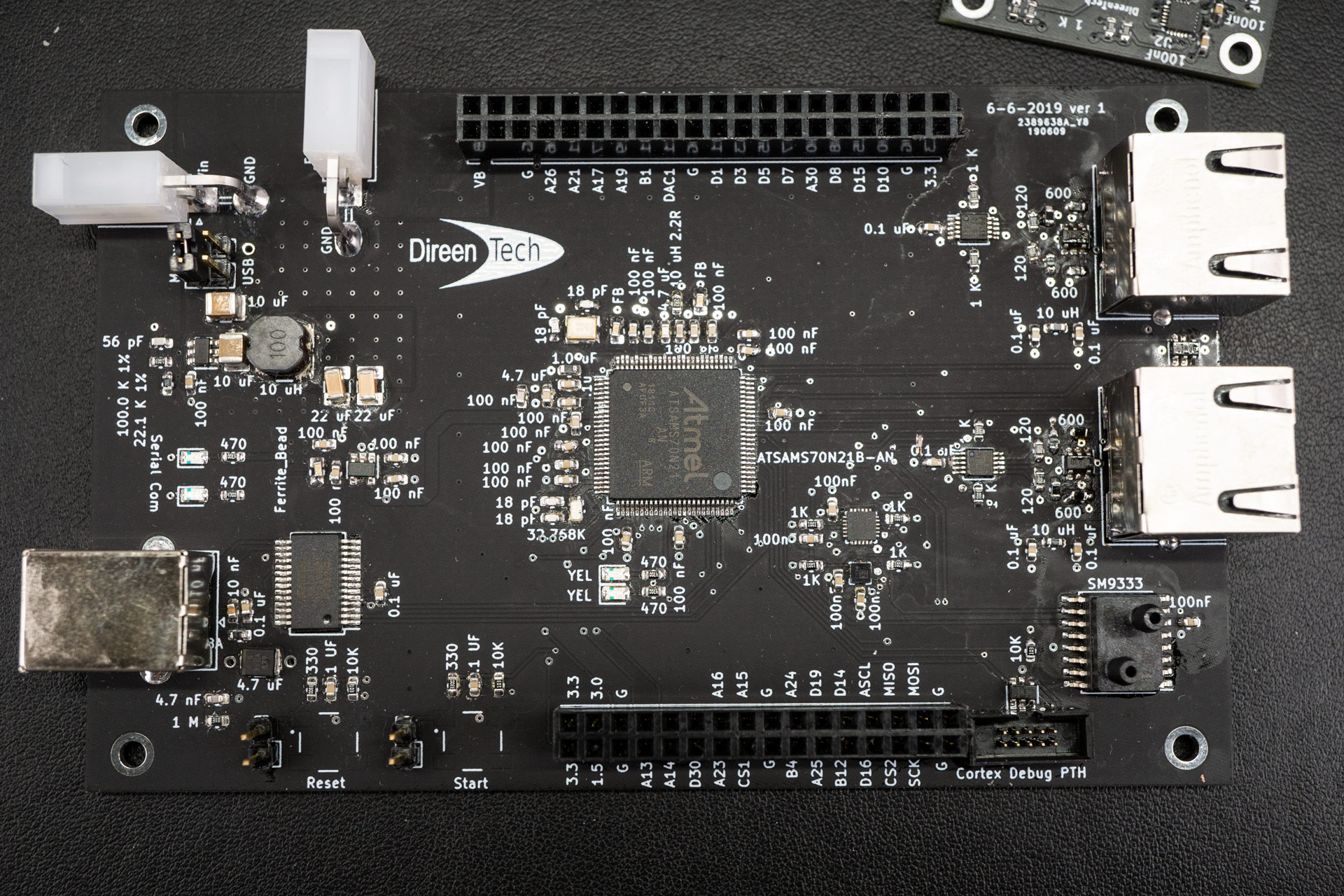
Here is the control board containing the Atmel SAMS70 chip. You may notice the poor soldering job. This is because I did it myself. We designed the board for a variety of projects, which is why there are a couple ports for hats we can add onto the board. This board has been a lot of fun to develop.
Atmel control board
Below is a picture of the control board and the AD9951s placed within a cheap metal box from Amazon. The aluminum box on the right containing the DDS modules was also bought on Amazon. I really like these little boxes for RF projects. Unfortunately, I didn’t put any filter on the ports of the DDS circuit boards so noise creeps out onto the ribbon cable 😐
Atmel board next to box containing the DDS modules
Inside the aluminum box I screwed the DDS modules into 3D printed stands that are glued to the aluminum bottom. This makes it easy to get the modules in and out for servicing.
DDS modules screwed into 3D printed stands
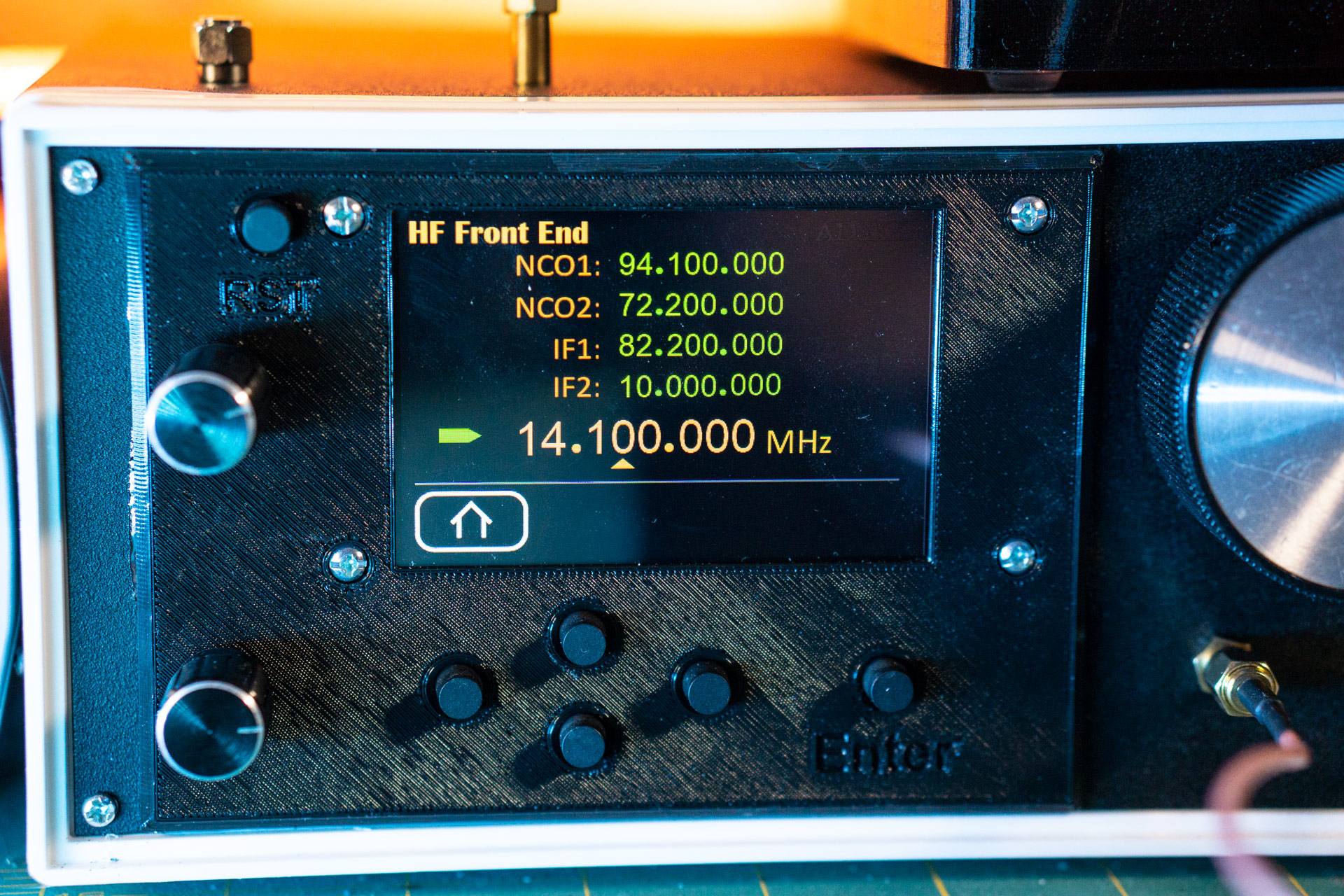
If you haven’t used a Nextion display in one of your projects yet, DO IT. It’s the easiest way to make a nice looking users interface (touch included) without having to write a mountain of code. The reason my display doesn’t look good (see below) is that my brother didn’t help. You can get an idea of how it should have looked if you visit his blog within this domain (http://www.direenworks.com). The particular Nextion display I used was a 3.5″ Enhanced version found on Amazon. I 3D printed a holder for it, some buttons, and rotary encoders, which was a lot easier and cleaner to do than just cutting places within the cheap metal box.
HF Front End display on Enhanced Nextion
I made two pages for the display. The page shown above is for controlling an HF front-end. The first NCO1 frequency is used to mix a signal up to a first IF and the second NCO2 is used to mix down to a second IF. The frequency at the bottom is the tuned frequency I’m interested in. I wanted this level of control so that I could play with different IF frequencies.
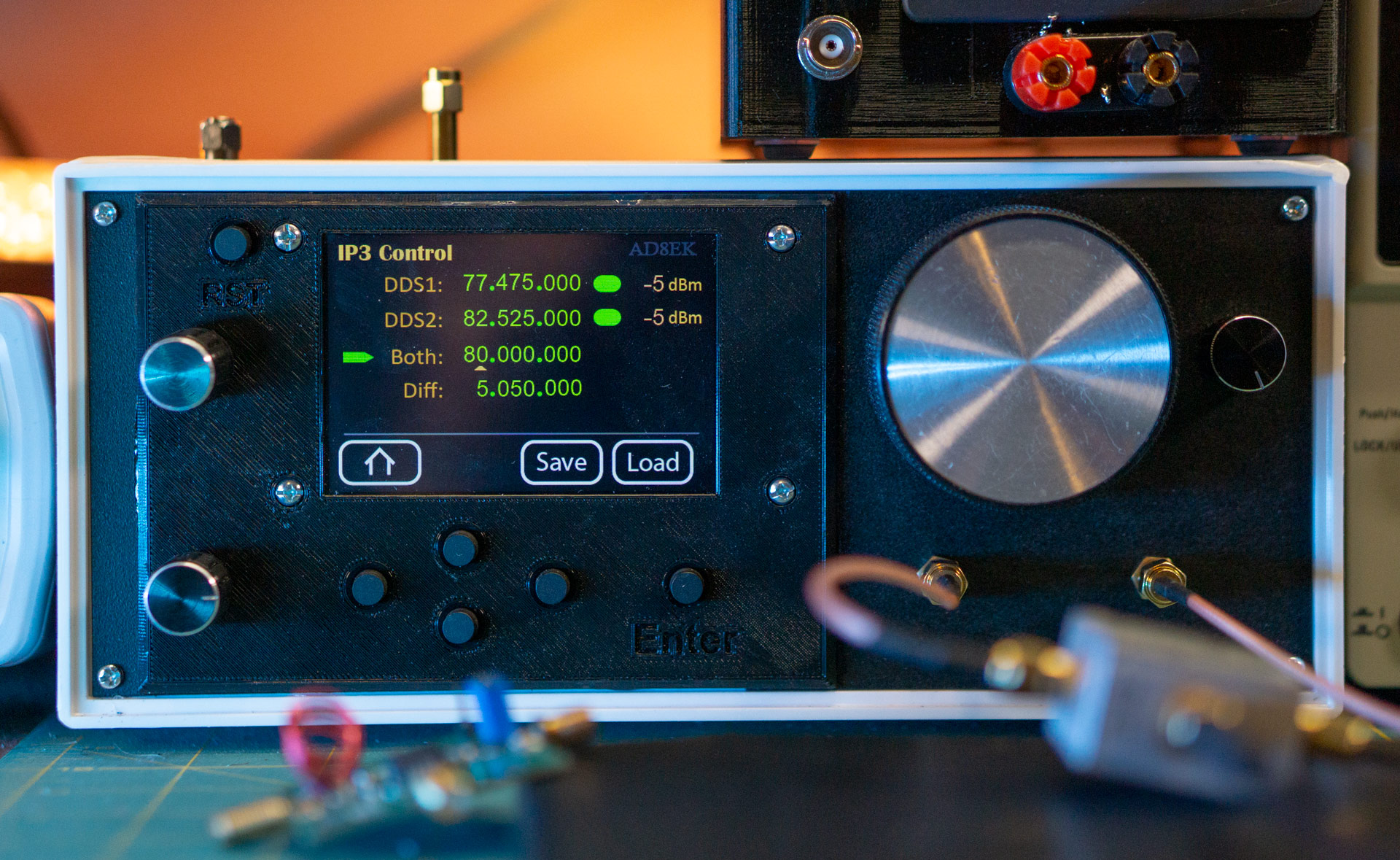
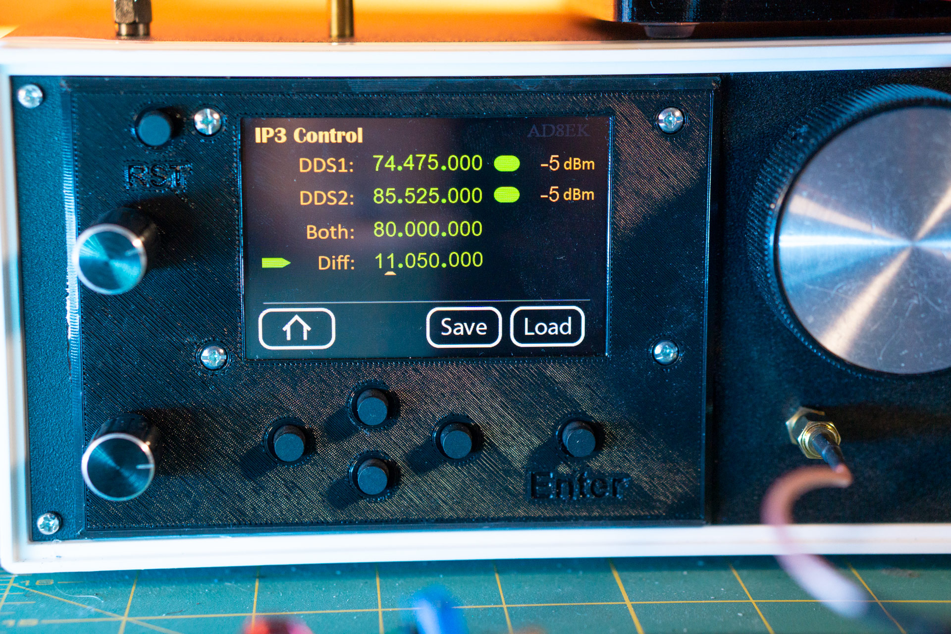
The second page is for controlling two tones at a time (see below). This is useful for IP3 measurements (measuring linearity of devices). The two DDS can be controlled independently or together and I can control their output power.
Here is a picture of the signal generator being used to measure OIP3. The device under test is a PGA-103 gain block and I measured OIP3 to be 34 dB. This was nice, because that’s what the datasheet said it should be. The controls of the signal generator make it really easy to choose frequencies I’m interested in and scrub through a reasonable amount of power levels.
I’m happy with this project. I now have a nice tool for generating a couple frequencies in the HF and VHF bands. I’m not sure if it was the most economical route to get what I wanted. I think all in all I spend between $250 and $350 to make it. But, I wanted to develop these pieces so I can use them in other radio projects. Fun stuff.
If you made it all the way to the bottom of this post, thanks for hanging out!
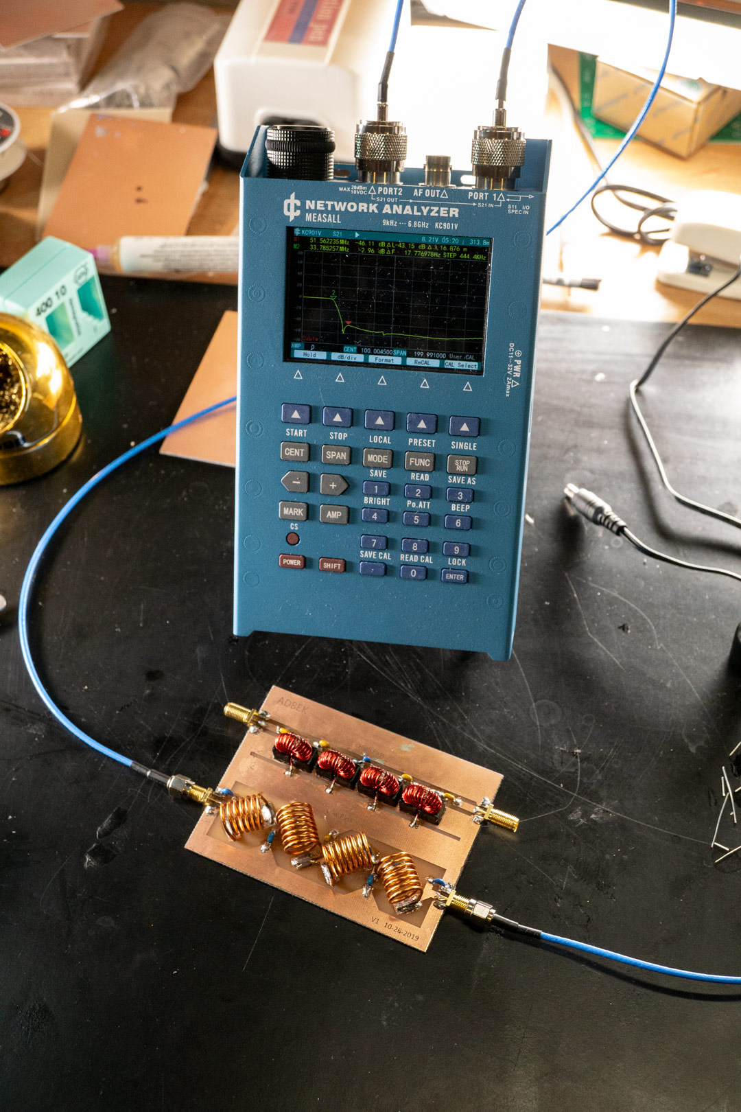
I’ve had it for about a year now and I can now say I truly love it. It’s from China and I took a real risk in buying it, but the product works great as a hobby VNA.
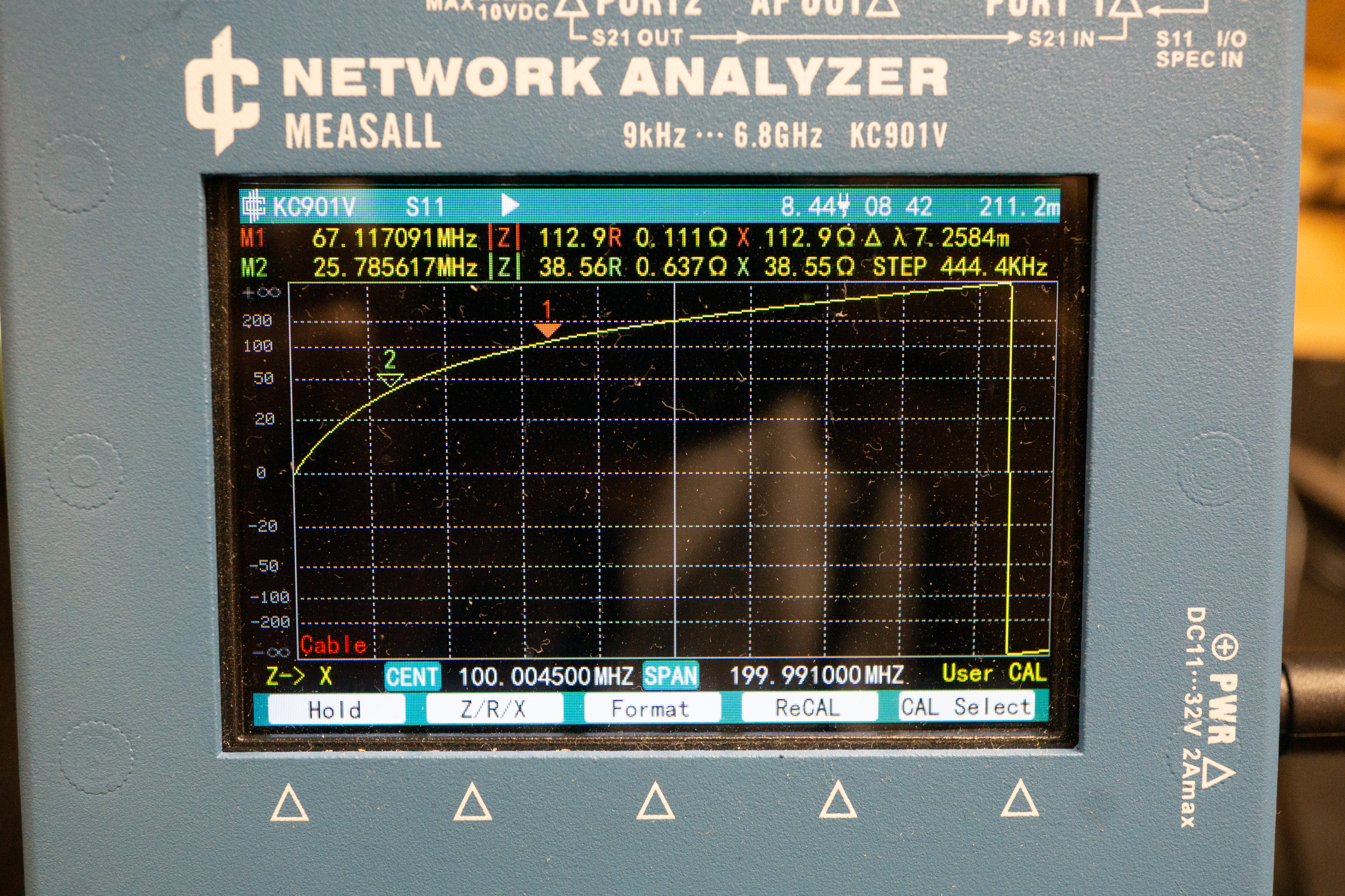
KC901V display
When I was shopping for a VNA, I spent a lot of time on eBay looking for used VNAs. In my price range I found a lot of old Keysight boxes that work up to 3 GHz. I was very tempted, but when I came across the KC901V I saw I could get a portable VNA that works up to about 7 GHz! I took a chance and bought it.
I have not been disappointed. There are a few quirks, but the interface works great and the metal body makes the whole thing feel solid. Support is good too! I had an issue with saving data to an SD card and e-mailed the guys; they were back to me within an hour and I got it worked out (it was simple and it was my fault).
Also, there is a nice ethernet interface which allows me to control the device from my computer. There is a caveat with it, you can only grab raw data that has not been corrected by calibration. This means you have to write something to do calibration for you. But, after a few hours, I figured out how to get MATLAB talking with the VNA so I can make nice graphs like the one below.
Before you rush to get one, you need to have in mind that the device does not do a full two port measurement. You measure either S11 or S21 at a time. Also, there is a bit of a matching problem when doing S21 measurements. To fix this I put 10 dB pads on both the connectors to get the ringing down. But, once you figure out how to deal with these issues, the unit works great for the price considering it works up to 6.8 GHz.